Hi Everyone,
As a follow-up to the semiconductor packaging market overview, this article provides an update on the broader semiconductor industry. When appropriate, I mentioned the impact of the industry trends on Kulicke and Soffa (KLIC; “K&S”). Note: This was originally published on April 12, 2021.
Please make sure to share this newsletter, share this post, or subscribe (if you have not already) if you like the content! You can use the buttons here to do so:
DISCLAIMER:
All investment strategies and investments involve the risk of loss. Nothing contained in this website should be construed as investment advice. Any reference to an investment's past or potential performance is not, and should not be construed as, a recommendation or as a guarantee of any specific outcome or profit.
Industry Overview
Market Opportunity and Dynamics
General Semiconductor Industry
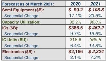
The overall market grew in 2020 despite COVID headwinds and the resulting supply chain disruptions. Semiconductor Applications Forecaster (part of IDC) reported that global semiconductor sales grew by 5.4% to $442B in 2020 despite the COVID headwinds. In my view, 2020 was set up for growth coming out of the 2019 cyclical downturn, but achieving growth given the macroeconomic landscape was impressive nonetheless. Broken out separately, DRAM and NAND grew 4% and 32.9%, respectively. IDCs 2021 forecast from February 2021 calls for 7.7% growth in chip sales to $476B. I see multiple tailwinds that are often discussed for the broader industry including 5G networks, Internet of Things (“IoT”), and Artificial Intelligence (“AI”), which are all still nascent in their overall development and will require a step-wise increase in processing intensity. IDC provided some information on their overall 2020 breakdown and 2021 forecast, which I have somewhat reverse-engineered here:
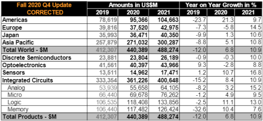
In mid-March, 1.5 months after IDC released its forecast, Worldwide Semiconductor Trade Statistics (“WSTS”) released the final 2020 chip sales figures along with its 2021 forecast. The image below is sourced from WSTS, revealing a breakdown by chip category. There are apparent differences between the two data sources, I lean towards WSTS. The organization reported 6.8% sales growth in 2020 to $440B; logic and memory led the industry last year. The expected acceleration in 2021 sales is a result of the supply constraints and chip shortages emanating from COVID disruptions and the aforementioned macro tailwinds. Total chip sales are expected to grow 10.9% above 2020 to $488B. The impact of IoT can be seen by sensors and analog chips leading the way this year.
In addition to total sales, tracking unit shipments is critical to understanding the performance of certain areas of the value chain – including, assembly equipment. The chart below from ICInsights displays annual IC unit shipments since the late 1970s, representing an 8.6% CAGR over that time period. I received the updated 2021 forecast containing actual 2020 shipments today (great timing). So, if I miss any edits of the unit shipment counts for 2021 in this write-up, remember that 2021 growth is expected to be 13.4%
Shipments accelerated from 2000-2007, fueled by the rise of the Internet until the global financial crisis (“GFC”) led to a cyclical decline in IC shipments in 2008 and 2009. Coming out of the GFC, smartphones had started taking hold, and unit shipments spiked by 25% in 2010, surpassing 705 billion devices. Another sharp increase of 12% occurred in 2017, which brought total shipments near one trillion, which the industry achieved in 2018. The expected acceleration in 2021 is in line with all of the commentary I have received from those in the industry and jives with the high fab utilization rates.
Shipments can also be viewed through the lens of total area shipped, measured in millions of square inches (“MSI”). Total wafer area shipments in 2020 increased by over 5% to 12.4 billion square inches over 11.8B in 2019. While not a direct indicator of the number of units shipped, semi.org’s forecast of record-high MSI shipment in 2022 with continued growth thereafter is another data point supporting overall industry growth.
Semiconductor Capital Equipment (“Semicap”)
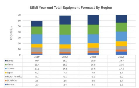
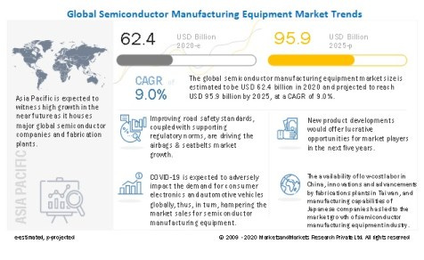
Total sales of semiconductor manufacturing equipment reached $59.6B in 2019 and are expected to have grown by 15.6% in 2020 to $68.9B according to SEMI. Strong growth in 2020 is expected to continue into 2021 and 2022, reaching $71.9B and $76.1B, respectively. The Semicap market can be bifurcated between the “Front End” and “Back End”; the Front End accounts for ~70% of the market with the Back End making up the remainder. Front End equipment relates to fabrication equipment, including photolithography, deposition, etching, cleaning, ion implantation, etc. Back End refers to assembly, packaging, and testing equipment. Kulicke & Soffa sits in this back-end, which is merging with the front-end. Separately, MarketsandMarkets forecasts the Semicap market to grow at a 9% CAGR through 2025, reaching $95.9B.
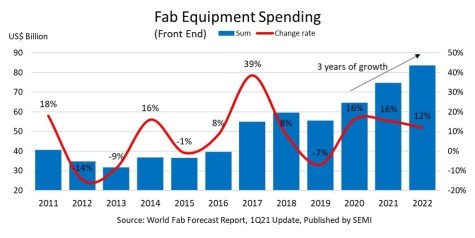
Wafer fab equipment (wafer processing, fab facility, photomask/reticle equipment) is estimated to have grown by 15% to reach $59.4B in 2020. This segment is expected to grow by 4% and 6% in 2021 and 2022, respectively. Foundry and logic account for ~50% of this market, as equipment churn/incremental spend is driven by the need to update facilities and processes with leading-edge equipment. NAND flash equipment stands out with 30% growth in 2020 (+$14B), with DRAM equipment expected to be the leader in 2021 and 2022. Separately, on March 16, 2021, SEMI reported a 16% increase in fab equipment spending in 2020, with continued robust growth expected for 2021 and 2022 resulting from “pandemic-inspired demand for electronic devices.” 2021 forecasted equipment spend is expected to increase by 15.5% in 2021 followed by slight deceleration in 2022 to 12%. This should equate to roughly $10B/year on incremental spend, reaching ~$80B by 2022.
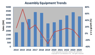
The Test equipment market is also expected to grow by 20% in 2020, reaching $6B. This market is also expected to experience healthy growth through 2022 due to demand from 5G and HPC end-markets. Assembly and Packaging equipment is “forecast to grow 20% to $3.5 billion in 2020, followed by 8% and 5% increases in 2021 and 2022, respectively, driven by advanced packaging applications.” VLSI is forecasting 10% growth in packaging equipment for 2021, with the market reaching $4.4B in 2023. Overall market trends provide a bullish backdrop for Kulicke & Soffa’s business as the leader in advanced packaging. The upside for the company is in the advanced packaging trends, which the company is starting to execute with its various design wins. The entire Semicap market is poised for robust growth for the next three years, with assembly equipment primarily driven by increasing utilization of advanced packaging solutions.
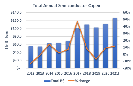
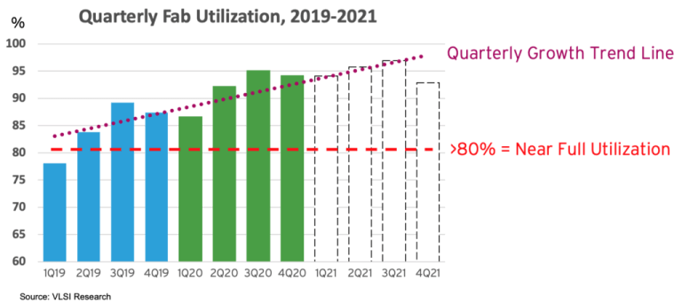
Semicap / SME companies’ performance is correlated to front-end CapEx spending. Historically, capital expenditures have followed periods of high fabrication capacity utilization as fabs and IDMs are forced to expand operations to meet demand. Fabrication capacity utilization will usually run above 80% in periods of high demand, with individual fabs running between 90%-100%. Capacity utilization above 90% is a key indicator of oncoming manufacturing expansion, which is a leading indicator for Semicap demand. However, adding capacity is a lengthy process due to the complexity of the plants and process lines in addition to the capital intensity. Connecting the dots between current high utilization and proliferating chip demand across industry verticals, fabs/IDMs will have to build out significantly more capacity in the oncoming years. This spending will filter down throughout the value chain, which is discussed further below.
Advanced Packaging Market
ResearchandMarkets estimates that the global Advanced Packaging market will grow from $29.4B in 2019 to $73.4B in 2027, representing a 12.1% CAGR. Detail on the AP technologies and demand drivers are provided below. The semiconductor industry must develop advanced packaging technologies to continue advancing chip performance, power, and size. Physical limitations and quantum mechanical dynamics serve as a cap on geometry scaling. Advanced Packaging provides a solution by building performance-enhancing capabilities into the package itself. As a result, the packaging process has moved from the back-end, as an afterthought, to the front-end and part of the overall design process. As a result, foundries and IDMs are starting to build out their own packaging capabilities – fighting for market share with OSATs. EET Asia provides a quote that encompasses the AP trend (emphasis mine):
“A new era of advanced packaging is at our doorstep. From advanced flip-chip and fan out technologies, now new and more advanced technologies are needed for assembly of double-sided SiP, as well new TCB and hybrid bonding solutions for complex heterogeneous packaging are required. This in combination with different carriers for Known Good dies (trays, TnR, reconstructed wafer) and other interposers (wafer, panel, substrate) opens opportunities for new, innovative and cost-effective, equipment that offer very high accuracy, high yield, and high speed. We see the demand for equipment that offers solutions to these industry demands growing strongly and have a clear focus on supplying such solutions in a timely way.”
Ruurd Boomsma, BESI’s CTO comments
The same tailwinds supporting the broader chip market apply to advanced packaging. Advanced Packaging is mostly used for the mobile and consumer markets currently, due to the smaller form factor. In addition to these trends, the need for more power-efficient consumer electronics and advanced chip architectures will be specific demand drivers for advanced packaging. However, there remains a possibility that OSATs and manufacturers will try to delay the transition to advanced packaging for as long as they can due to the higher initial and maintenance costs associated with AP. With that being said, the transition to advanced packaging for the high-end market is an inevitability (my opinion) as transistor scaling continues. Conversations with industry experts reveal that traditional wire bonders were priced around $60,000, but the “steppers” used for interconnect today cost “a few million dollars.“
Current State of the Industry
General Semiconductor Industry
All of the indicators I have been seeing indicate that 2021 and 2022 will be big years for the chip industry and specifically equipment companies. The last thing you all need is another take on the current chip shortage, the impact of which is being felt through many areas of the economy. Analyzing the confluence of factors is helpful to understand the inner workings of the global supply chain; however, it is more useful to look forward. The path forward starts with the current state of the industry. While the current backlog is partially a result of the demand shock resulting from consumer electronics sales and the work-from-home (“WFH”) paradigm, future demand will be heavily driven by AI, 5G, and IoT proliferation. This positive demand environment can be juxtaposed to the current and worsening long-term supply dynamics resulting from the difficulty of geometry scaling and increasing chip complexity discussed throughout this report. All of this points to a cyclical bull market within a secular bull market.
The latest industry data shows current capacity utilization of 96% as of March 2021, which makes sense given the aforementioned chip shortage. Fabrication capacity utilization is the percentage of the total available capacity that is used at a given time. IDMs and foundries are trying to catch up on a massive backlog of orders and have ramped production in response. In line with the market dynamic above, Taiwan Semiconductor (“TSMC”), Intel, Samsung, and others are announcing record levels of forthcoming capital expenditures (referenced below). However, even producing at 96% of capacity won’t bring market supply and demand into balance until some time in 2022. Techspot reports that Harlan Sur (J.P. Morgan analyst) estimates that supply is currently outpacing demand by 10-30%. He expects this imbalance to persist for the next three or four quarters; however, the situation wouldn’t be resolved at that point. The industry will need an additional one or two quarters before inventories reach normal levels. Piecing this all together results in a normalized market at some point in 2022.
Semiconductor fabrication capacity utilization has been trending higher since the beginning of 2019 and the start of a cyclical downturn for the industry. Utilization has been steadily rising, seasonally adjusted, since then except for the drop off in Q1 2020 due to COVID. But ramping utilization takes time due to process complexity and specialization of knowledge and equipment required for production. According to SIA, there can be up to 1,400 process steps to manufacture the wafer; each requires using highly sophisticated tools and machines. This results in a chip manufacturing process that takes up to 26 weeks, SIA explains:
Manufacturing a finished semiconductor wafer, known as the cycle time, takes about 12 weeks on average but can take up to 14-20 weeks for advanced processes. To perfect the fabrication process of a chip to ramp-up production yields and volumes takes even much more time – around 24 weeks. Then, once the fabrication process is complete, the semiconductors on the silicon wafer need to go through yet another stage of production known as back-end assembly, test, and package (ATP), before the chips are final and ready for delivery to the end customer. ATP can take an additional 6 weeks to complete. Therefore, the lead time, which is from when a customer places an order to receiving the final product, can take up to a total of 26 weeks. The table below provides some average times required in the chip fabrication process.
Semiconductor Industry Association
However, even if the industry continues operating at near 100% capacity, the current supply/demand imbalance has caused a 16-week lead time (time between order placement and order delivery) in March based on reporting from Bloomberg. This is the highest lead time since 2018, which has been categorized as the “danger zone” for inventory levels. It’s difficult to see this dynamic improving any time soon. Following the demand shock caused by the rapid growth in consumer electronic purchases resulting from the WFH movement, there is oncoming demand from the economic recovery throughout 2021. Coupled with continued headwinds on the supply side, including supply chain disruptions and idiosyncratic events (e.g. Samsung fab shutdown in Texas, Renesas fab fire), the forecast of a normalized by mid-2022 seems reasonable. Matthew Sheerin from Stifel also mentioned higher material costs as another constraint on supply.
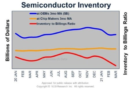
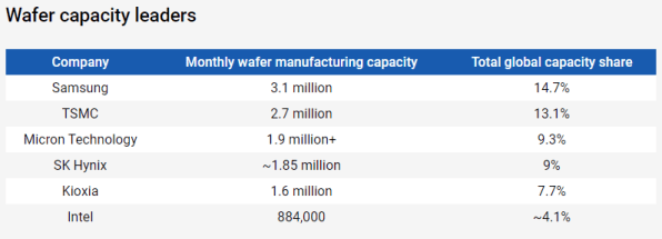
Even while running at above 90% capacity, inventory destocking relative to demand can be seen in the chart below. Inventory levels have come down slightly (in line with comments throughout the industry) and look to have stabilized but billings continue to move higher. This paints a picture of demand continuing to outpace supply. Rob Thubron states, “Exacerbating the issue has been the increasingly complex manufacturing process making chips more difficult to produce, the larger number of chips in every device, logistical problems, and package shortages. The China/US trade war saw companies trying to stockpile chips in advance, putting further pressure on manufacturers.” As a result, wafer manufacturers will need to keep up with high production levels and expand capacity. The current capacity picture can be seen below:
Semiconductor Packaging Market
Structural Changes – Advanced Packaging
Chip manufacturers are developing their own packaging/back-end solutions. As an example, TSMC developed leadership in the space by developing a leading-edge advanced packaging platform for its customers. These solutions include fan-out (InFO) to 2.5D Si interposer (CoWoS), to 3D SoIC, all of which contribute to their 3rd or 4th place positioning among OSATs for just its packaging business. But it is important to point out that TSMC and other foundries will only provide advanced packaging solutions, not traditional packaging like wire bonding. Wire bonding will always have a presence in the industry but will stay with the OSATs. Due to the commoditized nature of traditional wire bonds, OSATs could be relatively indifferent to the equipment they used; allowing these customers to play the equipment providers off each other. K&S noted the resulting lower margins on its traditional wire bonding business. This provided a better overall pricing environment for the OSATs, which was helpful given the low margins. However, since advanced packaging is involved on the front-end and much more complex than traditional methods, the pricing environment is also different.
“And the thing is that people couldn’t realize that if you offload Moore’s law into packaging, packaging has to cost more. There are examples where the packaging is extreme examples, too, but the packaging cost more than the silicon.”
JCET Group Manager, Interview
Industry insiders are confident in advanced packaging’s continued and growing role given broader technological advancements and the capabilities AP provides. The same JCET Group manager commented, “So 6G used to be the millimeter-wave with 150 gigahertz operations. So the future product, they will all be based on very advanced packaging because you need AI accelerators, image processors. You need high bandwidth memory, processors. So CPU, 64 gigahertz products modem for millimeter-wave modem, 5G, 6G.“
While the wire bonding outlook in the medium term is very bullish, the industry also believes that there is a structural “new normal” coming due to increased competition. This will be in light of the industry adding significant capacity over the next two to three years as is expected. The competitive landscape may lead to further consolidation following ASE’s acquisition of SPIL, which was formerly the fourth largest OSAT.
Recent Underinvestment
In addition to the growing prevalence of advanced packaging, Kulicke & Soffa will benefit immensely from what I believe is an oncoming increased investment in wire bonding resulting from previous years of underinvestment in wire bond capacity. An interview with ASE (#1 OSAT; KLIC #3 customer) illuminated the opportunity for Kulicke & Soffa (emphasis mine):
ASE is pretty consistent. But in terms of wire bond, we haven’t added a ton of wire bond capacity because the margins weren’t that good. Years ago, and again, I think Amkor came back and retooled a lot of their lead frame-based packages to larger chip sizes and stuff, the high matrix tooling and stuff where they could become more profitable. And that worked out well for them for a while because they captured a lot of the wire bond, because a lot of this stuff isn’t going anywhere… You can do a flip chip to your fan or some different packages, but you’re going to pay more. So no one’s added capacity in the last couple of years without contributing to price right now.
I think we’ve got over 1,200 wire bonders on the order. We’re adding 10% in Q1 (2021), 8% in Q2 (2021). So we are expanding wire bond capacity. But we’re doing it because we have loading commitments and long-term commitments from our customers. So wire bond capacity is pretty fungible. You can use it for a QFN or you can use it for an SLIC. So there’s not a huge amount of risk.
ASE, Interview
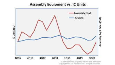
Given that assembly equipment sales are correlated to IC unit shipments, the recent underinvestment makes sense a priori. However, this is a critical claim that needs to be verified. The graphic below shows how leveraged assembly equipment sales are to integrated circuit unit shipments. Investment in assembly equipment experienced a deep decline in 2019 as the semiconductor market experienced a trough in its industry cycle. The bear market in 2019 was followed by COVID in 2020, a further drag on IC shipments and thus equipment sales. Underinvestment the past two years has created capacity constraints, creating a scenario that should result in rapid sales growth over the next one to two years. The result has been a wirebonding shortage unlike anything industry participants have seen in 20 years, expanded on below.
ASE spent ~$1.6 billion on capacity expansion in 2020; a lot of which was for wire bond with the majority for advanced packaging. To further that point, ASE group COO Tien Wu stated that the company “will see its wire-bonding capacity run at full utilization and remain short of demand through the end of 2021, and up to 90% of clients have signed two-year contracts for capacity support.” This underinvestment and oncoming spend by ASE is actually an industry-wide phenomenon, as noted by ASE’s COO on their earnings call (emphasis mine):
However, given the 2020 capacity crunch, I believe all of our competitors are placing order for all of the equipment that are required to meet customer demand.
Dr. Tien Wu, COO of ASE Technology Holding – Q4 2020 Earnings Call
Shortages and Long Lead Times
The structural changes and recent underinvestment in wire bonding, coupled with the spike in demand over the past year, have led to a wire bond shortage. This massive shortage puts K&S in an even more important position in the overall value chain. This is the biggest shortage in at least 20 years, as mentioned below (emphasis mine):
I’m sure you’ve probably heard that right now, there’s a huge worldwide wire bond shortage. That’s just insane. I’ve never seen it in 20 years in the industry where customers weren’t getting enough wire bond.
ASE, Interview
ASE elaborated on the state of the wirebonding market in their latest earnings call. Note the confirmation of 1,200 wire bond additions from the interview comment above, except the COO states that the 1,200 is only confirmed delivery. They want to double their capacity this year but are reliant on the machinery lead times, from K&S:
The first question is the demand has not slowed down at all. And the machinery lead time is getting longer. That’s why we’re confident that the wire bonder capacity will remain to be tight to the end of this year, at least, if not longer. In terms of the number of wire bonders we’re adding, I think last year we have 1800 (additions), and this year we believe we will add to similar number of units. Right now we have confirmed delivery of 1200. And we’re working on the other. In terms of the wirebonder tightness…is a combination of demand has not slowed down, as well as machine lead time. And it’s not just wire bonder, its the whole line balance.
Dr. Tien Wu, COO of ASE Technology Holding – Q4 2020 Earnings Call
Dr. Tien side-stepped a question that directly referenced K&S, but confirmed that the long lead times apply to many of their vendors and equipment used. In ASE’s Q3 2020 earnings call, the company estimated that the wire bond shortage would persist through Q2 2021. It is now extending this expectation through the end of 2021 at a minimum. They also increased the machinery delivery lead time (how long they have to wait) from 6-8 months to 6-9 months, the environment is not improving yet.
Amkor (#2 OSAT) has echoed the same message as ASE, as Amkor’s VP of wirebond BGA products stated, “We are seeing capacity tight pretty much across the board.” To focus only on wire bonds would be missing the bigger picture; shortages are seen in manufacturing capacity, certain packaging types, key components, and equipment. The equipment shortage means more orders for Kulicke & Soffa, specifically its two main business lines. The spot shortages in packaging began to emerge in late 2020; both wirebond and flip-chip capacity is expected to remain tight through 2021. In addition to the tight capacity, delivery lead-times for wire bonders and other equipment have stretched further. Lead frames and substrates are also in short supply and are core components used in packaging.
Given that wire bonding accounts for 75%-80% of all packaging today, based on interconnect methodology, KLIC should be one of the primary beneficiaries of the current market environment. Even when the market stabilizes in 2-3 years, the increased proportion of memory dies that are stacked will continue to drive demand for advanced wire bonding services. ASE stated in the Q3 2020 conference call, “in this particular cycle, it’s not just the volume. It’s also the number of dies, the number of wires, as well as the complexity.”
Flip-chip mounting is also experiencing above-average demand as an advanced packaging process. Amkor expects flip-chip capacity to continue running at a high level of utilization through 2021, with equipment lead times “greater than 2x what we typically experience.” Roger St. Amand, Sr. VP at Amkor, elaborates that “Based on available forecasts, we expect this trend to continue through 2021, and into 2022, driven by higher demand in the communications, computing, and automotive market segments. In general, we are seeing this trend across all flip-chip package technologies.”
Demand Drivers
In summary, the semiconductor capital equipment market demand, on the whole, is driven by upstream capital expenditures, among other things. Rapid buildouts of new foundries and foundry expansions to add broader industry capacity require more and cutting-edge tools. Most recently, Intel announced its plan to invest $20B to build two leading-edge fabs in Arizona, both expected to go online by 2024. Not to be outdone, on March 31st Taiwan Semiconductor announced that it plans to invest $100B in just the next three years to expand capacity. All of this CapEx is revenue for Semicap companies. DRAM content required by the automotive end-market and a proliferating consumer electronics market, driven by 5G, provide two additional tailwinds. Capital intensity and complexity will only continue as geometry scaling continues to be a goal within the industry and supplemented by advanced packaging technologies to keep pushing the limits of IC functionality. Finally, demand for semiconductor chips in the form of more intensive computational power, connectivity, and memory requirements will persist for many years due to growth in AI, edge network, and server applications.


